1004,West-CBD,No.139 Binhe Rd,Futian District,Shenzhen, China Post Code:518048
 +86-18682200597
 sales@szhaiwang.com


1004,West-CBD,No.139 Binhe Rd,Futian District,Shenzhen, China Post Code:518048
+86-18682200597
sales@szhaiwang.com


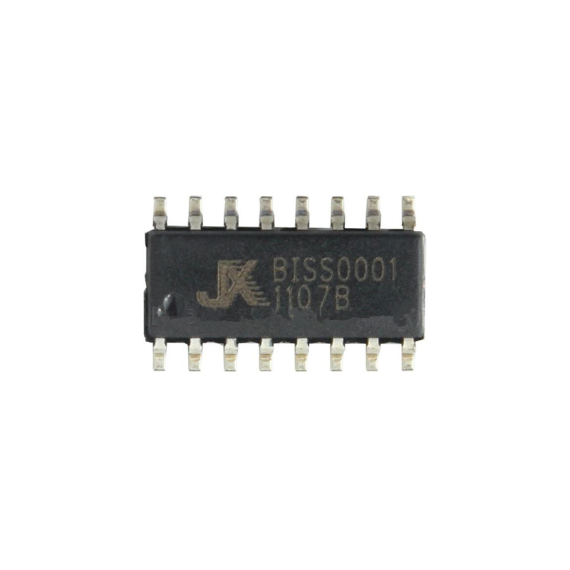
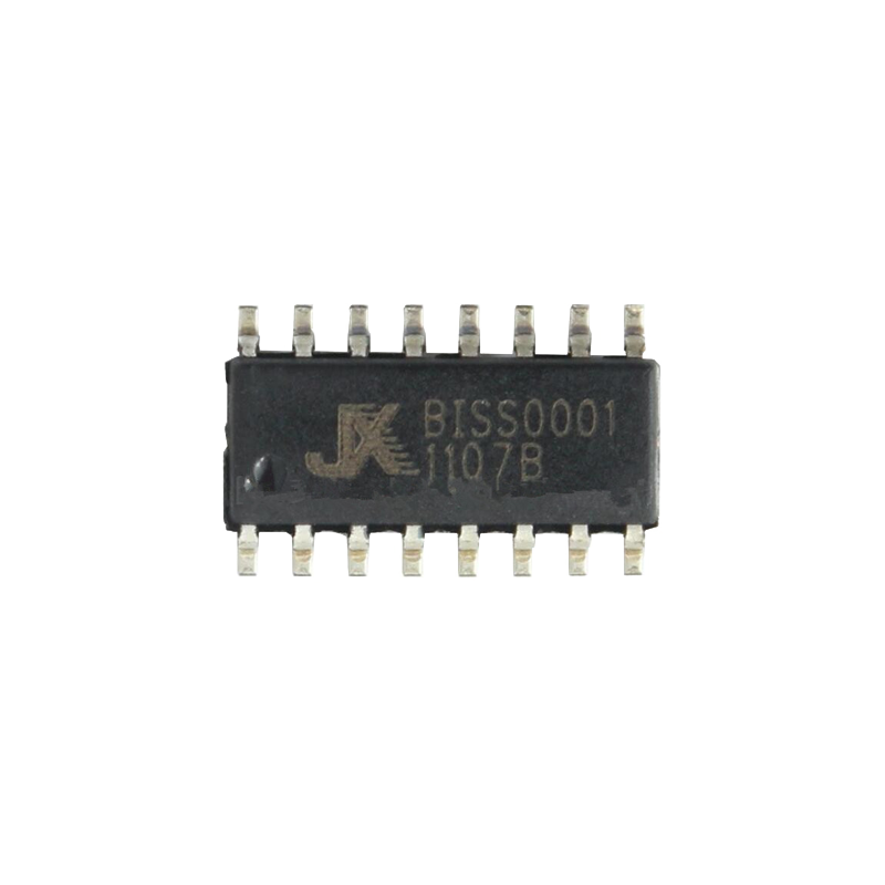
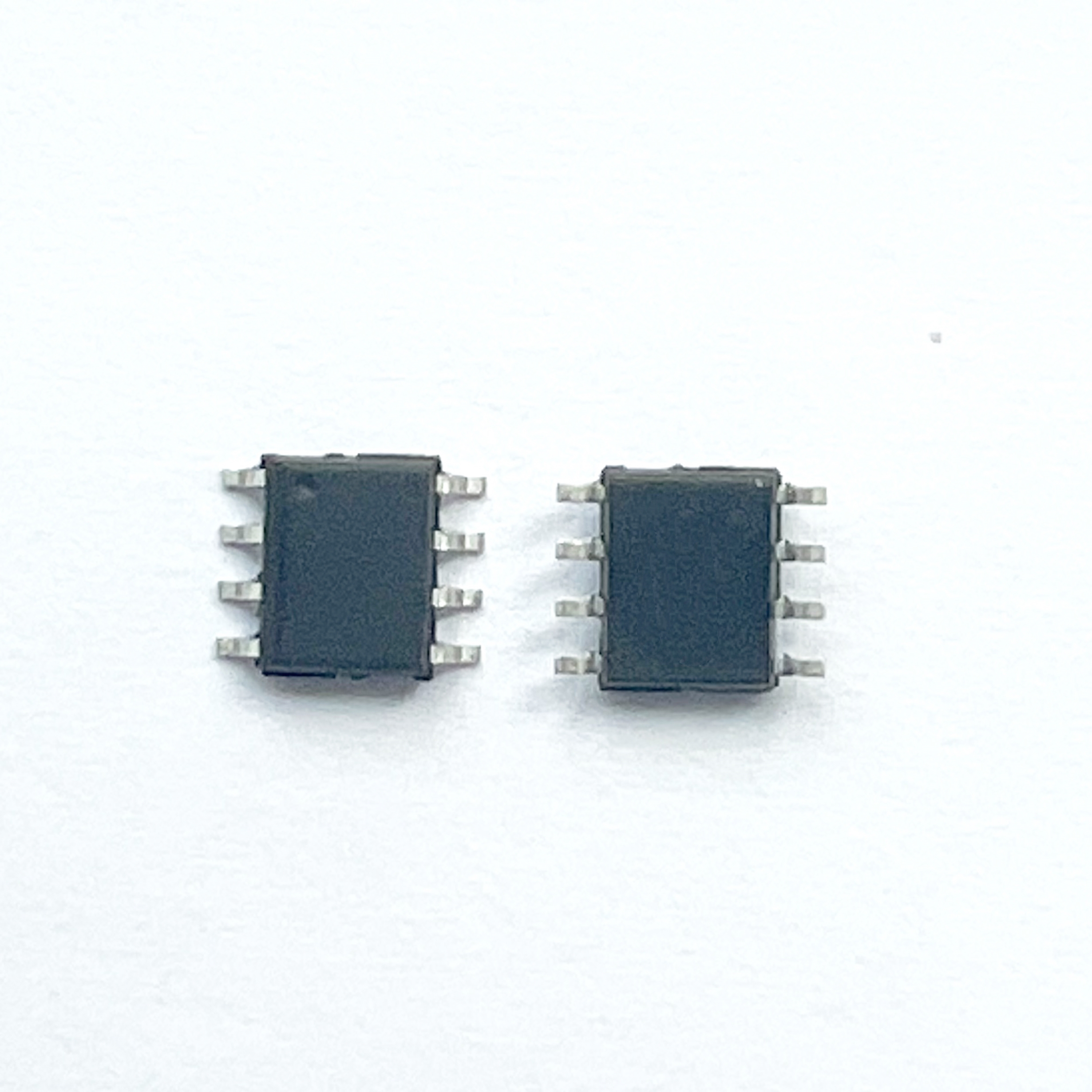
BISS0001 is sensor signal processing integrated circuits which has high performance. It matches with pyroelectric infrared sensor and a few external components to constitute a passive pyroelectric infrared switch. It can automatically open all kinds of flashlight lamps, fluorescent lamp, buzzers, automatic doors, electric fans, dryers and automatic sink devices, especially in sensitive areas like enterprises, hotels, shopping malls, warehouses,garage, corridor and so on.
 Online consultation
PIR Detecting Control IC
")
Brief
BISS0001 is sensor signal processing integrated circuits which has high performance. It matches with pyroelectric infrared sensor and a few external components to constitute a passive pyroelectric infrared switch. It can automatically open all kinds of flashlight lamps, fluorescent lamp, buzzers, automatic doors, electric fans, dryers and automatic sink devices, especially in sensitive areas like enterprises, hotels, shopping malls, warehouses,garage, corridor and so on. it's also widely used in safety area where there are automatic lighting, illumination devices and alarm systems.
Feature
1. Professinal CMOS mixed-signal integrated circuits.
2. With independent high input impedance of the operational amplifier which can match with a variety of sensors to signal and processe.
3. Bidirectional discriminator which can effectively resistance to interference. 4 Built in delay time timer and block time timer.
5 New structure, stable and reliable performance and wide adjustment rang.
6. Built-in reference voltage.
7. Operating voltage: 3-5V
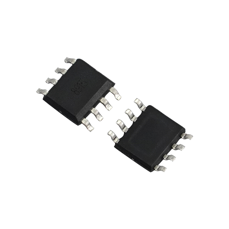
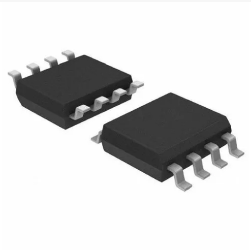
8. 16 feet DIP and SOP encapsulation.
Application
Used for a variety of sensors and delay controller
Limit Parameter(Vss=0V)
1. Power voltage:-0.3V ~6V
2. Input voltage:VSS-0.3V ~VDD+0.3V(VDD=6V)
3. leading-out terminal maximum current:±10mA(VDD=5V)
4. Operating temperature:-10℃~+70℃
5. Storage temperature:-65℃~+150℃
Electric Parameter
Symb ol | Parameters | Test Conditions | Value | Unit | ||
Min | Max | |||||
VDD | Operating vol. rang | — | 3 | 6 | V | |
IDD |
Operating current | Outp ut No Load | VDD=3V | — | 50 |
uA |
VDD=5V | — | 100 | ||||
Vos | Input offset voltage | VDD=5V | — | 50 | mV | |
Ios | Input offset Current | VDD=5V | — | 50 | nA | |
Avo | open-loop voltage gain | VDD=5V,RL=1.5M | 60 | — | dB | |
CMR R | common mode rejection ratio | VDD=5V,RL=1.5M | 60 | — | dB | |
VYH | op-amp output high level |
VDD=5V,RL=500K,1/2 VDD | 4.25 | — |
V | |
VYL | op-amp output low level | — | 0.75 | |||
VRH | Vc input high level | VRF=VDD=5V | 1.1 | — | V | |
VRL | Vc input low level | — | 0.9 | |||
VoH | Vo output high level | VDD=5V,IoH=0.5mA | 4 | — | V | |
VoL | Vo output low level | VDD=5V,IoL=0.1mA | — | 0.4 | V | |
VAH | A end input high level | VDD=5V | 3.5 | — | V | |
VAL | A end input low level | VDD=5V | — | 1.5 | V | |
")
Foot Function
Item | I/O | Function specification | |
1 |
A |
I | Repeatable triggered and non-repeatable trigger control end. A = "1" is the trigger while A = "0" is non- repeatable |
2 |
VO |
O | The control signal output. It is effective trigger when the Vo is triggered by the dance edge on Vs jump from low level to high level . It is low level state when the Tx output delay time is beyong and the Vs turn to Vo |
3 | RR1 | -- | Adjustment end of output delay time TX |
4 | RC1 | -- | Adjustment end of output delay time TX |
5 | RC2 | -- | Adjustment end of trigger block time Ti |
6 | RR2 | -- | Adjustment end of trigger block time Ti |
7 | VSS | -- | Operating power negative end |
8 |
VRF |
I | The reference voltage and reset input end which usually is connected to the VDD. It can make the timer reset with connected to the "0". |
9 |
VC |
I | Trigger ban end. When Vc < VR, it bans trigger; When VC > VR , it allows trigger. VR material 0.2 VDD |
10 |
IB |
-- | Operational amplifier bias current settings end.The RB is connected to VSS end, then RB value is about 1 M Ω |
11 | VDD | -- | Operating power positive end. It is 3-5V. |
12 | 2OUT | O | The second operational amplifier output end |
13 | 2IN- | I | The second operational amplifier negative output end |
14 | 1IN+ | I | The first operational amplifier positive input end |
15 | 1IN- | I | The first operational amplifier negative input end |
16 | 1OUT | O | The first level operational amplifier output end |
Inner Structure Diagram
")
1. Non-trigger working way waveform on each point
")
2. Trigger working way waveform on each point
")
BISS0001 Reference Wiring Diagram
")
Electric Parameter
Symb ol | Parameters | Test Conditions | Value | Unit | ||
Min | Max | |||||
VDD | Operating vol. rang | — | 3 | 6 | V | |
IDD |
Operating current | Outp ut No Load | VDD=3V | — | 50 |
uA |
VDD=5V | — | 100 | ||||
Vos | Input offset voltage | VDD=5V | — | 50 | mV | |
Ios | Input offset Current | VDD=5V | — | 50 | nA | |
Avo | open-loop voltage gain | VDD=5V,RL=1.5M | 60 | — | dB | |
CMR R | common mode rejection ratio | VDD=5V,RL=1.5M | 60 | — | dB | |
VYH | op-amp output high level |
VDD=5V,RL=500K,1/2 VDD | 4.25 | — |
V | |
VYL | op-amp output low level | — | 0.75 | |||
VRH | Vc input high level | VRF=VDD=5V | 1.1 | — | V | |
VRL | Vc input low level | — | 0.9 | |||
VoH | Vo output high level | VDD=5V,IoH=0.5mA | 4 | — | V | |
VoL | Vo output low level | VDD=5V,IoL=0.1mA | — | 0.4 | V | |
VAH | A end input high level | VDD=5V | 3.5 | — | V | |
VAL | A end input low level | VDD=5V | — | 1.5 | V | |
We are devoted to develop and manufacture the energy saving and intelligent products.,World knows our creation, New intelligence betters life


About Us

Product
News
Service

szhaiwang4@hotmail.com
+86-18682200597
sales@szhaiwang.com